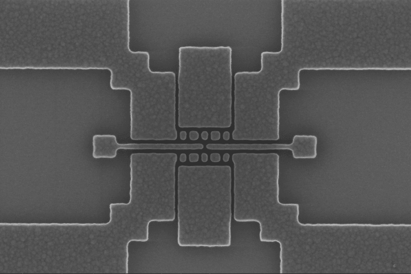
World First: Imec's Quantum Dot Qubit Using High NA EUV
On May 19, 2026, at ITF World, imec announced a milestone: the first quantum dot qubit device fabricated using High NA EUV lithography. The device features a functioning array of qubits with gate gaps of barely 6 nanometers—enabled by ASML's most advanced lithography system.
Why This Matters for Quantum Computing
Quantum computers promise exponential speedup for problems like drug discovery and materials simulation. But a useful quantum computer needs millions of connected qubits with low error rates. Silicon quantum dot spin qubits, which confine a single electron in a silicon nanostructure and use its spin state to store quantum information, are considered a strong candidate for industrial scaling because they leverage existing CMOS manufacturing.
The Technical Leap: 6nm Gate Gaps
Coupling strength between neighboring quantum dots increases exponentially as the gap between them shrinks. Imec's team, led by project leader Sofie Beyne and program director Kristiaan De Greve, used High NA EUV lithography to pattern gaps of just 6nm between the plunger and barrier gates that control the qubits. This is a dramatic improvement over previous demonstration devices and is critical for reducing environmental noise.
CMOS Compatibility: The Key to Scaling
Imec's previous results already showed that CMOS-compatible processes can yield low charge noise and stable qubit operation. By adding High NA EUV lithography, the focus shifts from individual lab devices to 300mm fab-compatible, reproducible quantum bits. "We can leverage decades of semiconductor innovation and reuse the entire ecosystem of silicon scaling," Beyne explained.
High NA EUV: Not Just for Classical Chips
High NA EUV is known as the enabler for sub-2nm logic and high-density memory, fueling AI and high-performance computing. This demonstration shows it also plays a pivotal role in quantum hardware. The same lithography that prints billions of transistors for classical chips can now pattern the nanoscale features needed for quantum dot qubits.
What This Means for Developers
For engineers working in quantum computing, this is a clear signal that silicon spin qubits are on a path to manufacturability. The ability to use standard semiconductor fab tools reduces the cost and complexity of scaling. While the qubit count is still modest, the reproducibility and uniformity enabled by High NA EUV lithography address one of the biggest hurdles in quantum hardware.
Next Steps
Imec plans to continue refining the qubit design and integration, aiming to demonstrate larger arrays and improved coherence times. The industry should watch for yield data and error rate benchmarks on these 300mm-fabricated devices. For now, the proof-of-concept validates that industrial lithography can meet the stringent requirements of quantum dot qubits.